Our team endeavors to design strategic & advanced electronic materials for future electronics, optoelectronics, and sensor devices & chips, especially in the fields of advanced sensing & detection materials, wide band gap & ultra-wide band gap semiconductor materials, advanced photonic & photoelectronic materials, low-dimensional & nano-sized electronic materials, advanced sensing/photoelectronic/electronic devices & chips, as well as advanced electronic materials calculation & design, etc.
Research interest
1. Gas sensing technology:
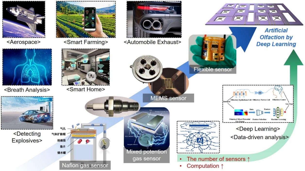
We developed a set of low-power-consumption, mini-size, integrated, intelligent and high-performance gas sensors by the fusion of nanomaterials technology, micro/nano processing technology and artificial intelligence algorithm, for the applications of environmental monitoring, industrial production, safety protection, aerospace, breath analysis, smart home & farming, and other fields. These gas sensors mainly include MEMS semiconducting-type gas sensors, solid electrolyte-type gas sensors, fuel cell-type gas sensors, flexible & wearable gas sensors, etc.
2. Biosensing technology:
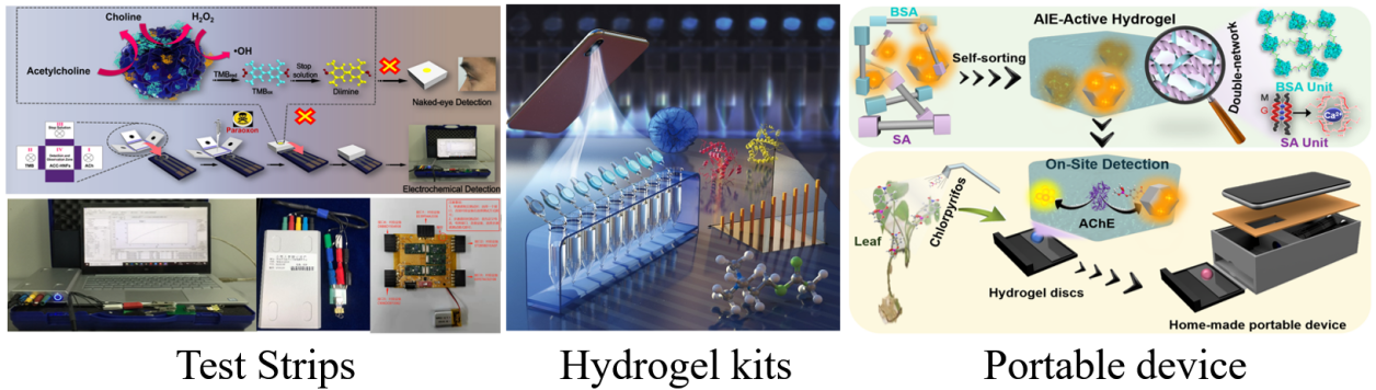
We proposed a composite assembly or surface modification strategy to improve target recognition and amplify the output signal, and constructed a new kind of highly sensitive enzyme-based fluorescence sensor to solve the problem of low detection sensitivity of biosensors. Furthermore, we used printed electronics and 3D printing technology to integrate paper-based chips and test kits, and build portable devices to realize on-site monitoring of biomarkers.
3. Flexible pressure sensor:
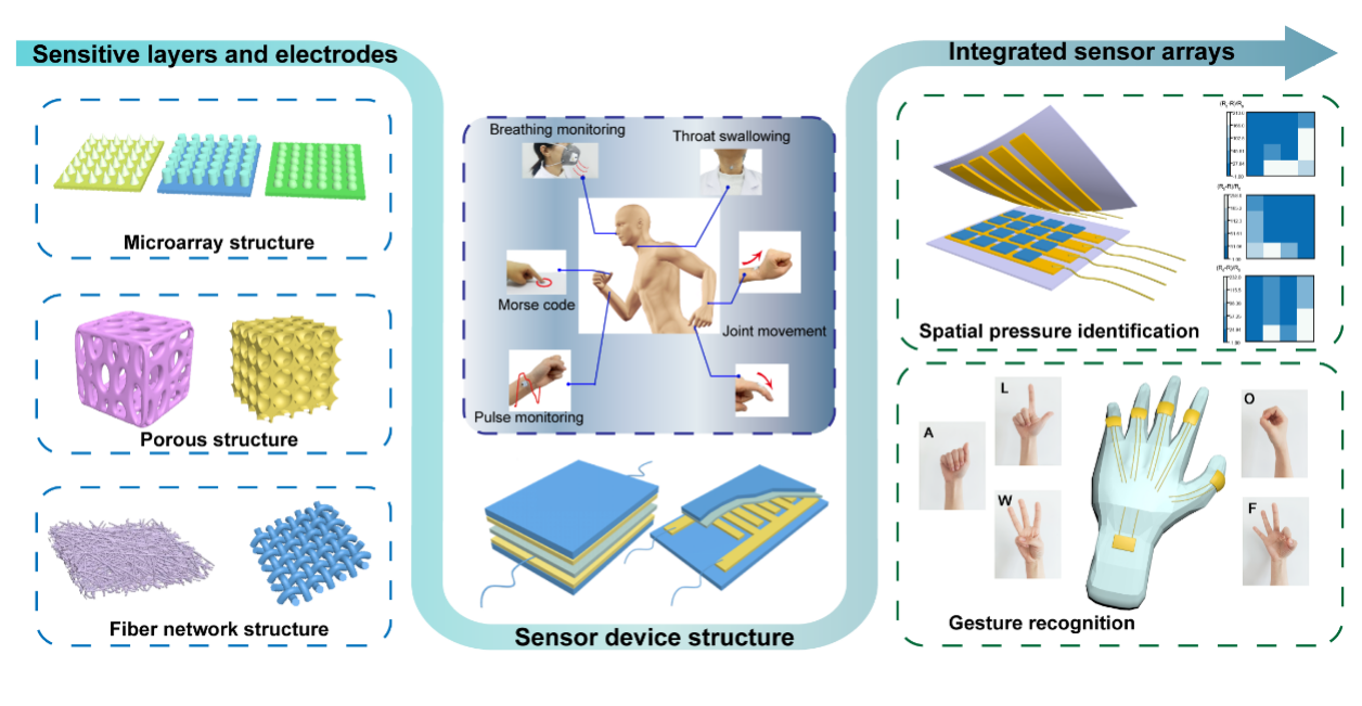
Focusing on the fields of electronic skin, human-computer interaction, health monitoring and healthcare, we developed a series of sensitive layers and electrode layers with micro/nanostructures (such as micro arrays, porous structures, fiber network structures, etc.) to construct flexible wearable pressure sensors with high sensitivity, wide detection range, and fast response characteristics, achieving real-time monitoring of human pulse, respiration, swallowing and joint movement. Furthermore, we used integrated flexible pressure sensor array and artificial neural networks for realizing spatial large area pressure distribution recognition, gesture recognition, and pressure distribution visualization.
4. Light-emitting devices based on nitride semiconductor:
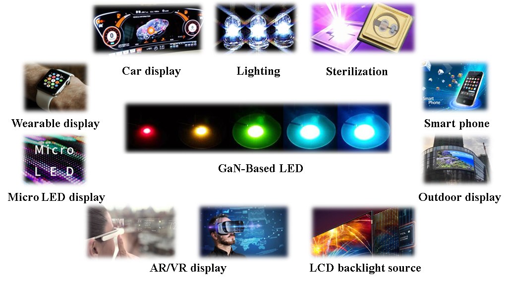
Epitaxial growth of nitride films with large mismatch and strong polarization. Fabrication of high-efficiency visible and ultraviolet LEDs. Develop approaches to control the polarization electric field in nitride quantum wells grown on the c-axis so as to realize weak polarization electric field LEDs with high efficiency and wide modulation bandwidth.
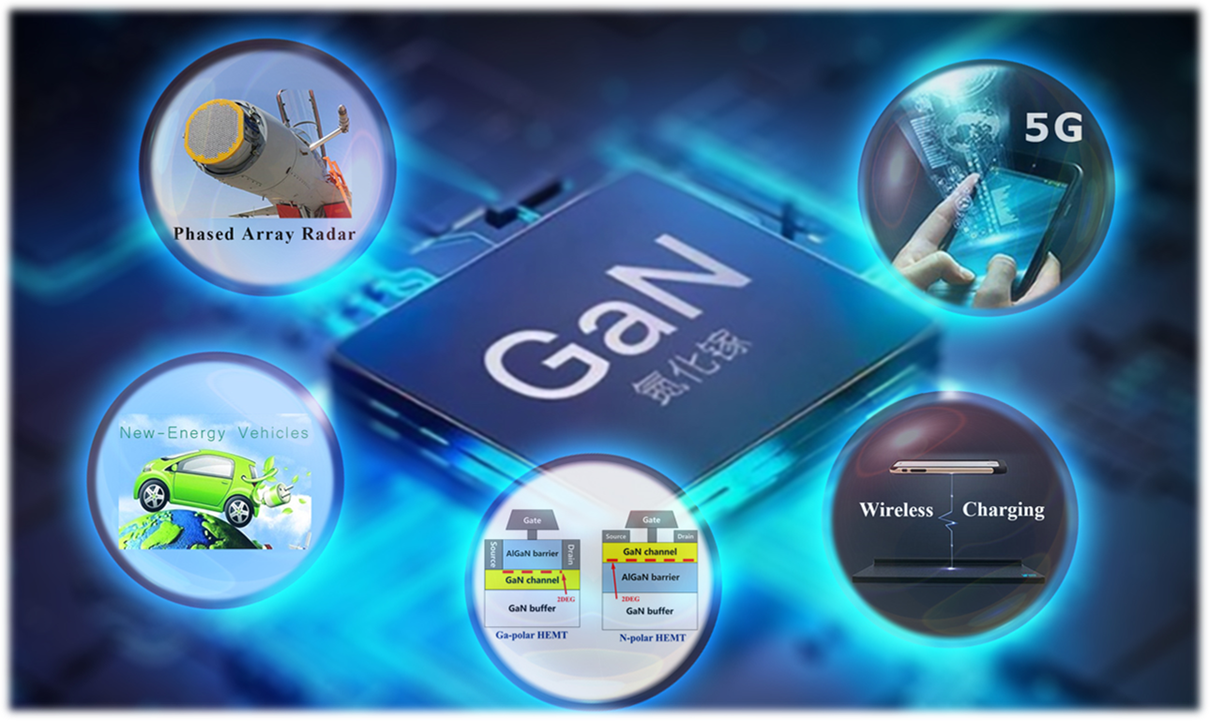
5. Electronic devices based on nitride semiconductor:
Research on key issues related to the material growth, structure design, and device fabrication of nitride high-electron mobility transistors (HEMTs) with high-frequency and high-power, such as controllable growth of high-resistance nitride films, design and epitaxial growth of GaN/AlGaN heterojunction structures with high electrical characteristics, and device processes like surface treatment, metal-semiconductor contact, sidewall passivation and so on.
6. Physics on nitride semiconductor materials and devices:
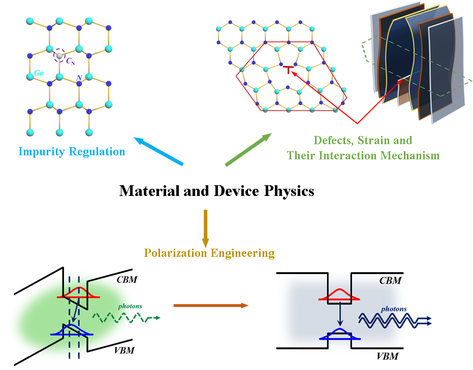
Study the defects, strain and their interaction mechanisms of nitride semiconductor materials. Investigate the impurity regulation mechanism of nitride semiconductor materials. Study the carrier transport, reliability and failure mechanism of nitride semiconductor devices. Develop the band engineering and polarization engineering of nitride semiconductor.

 Home
Home